


PCB Layout and Analysis


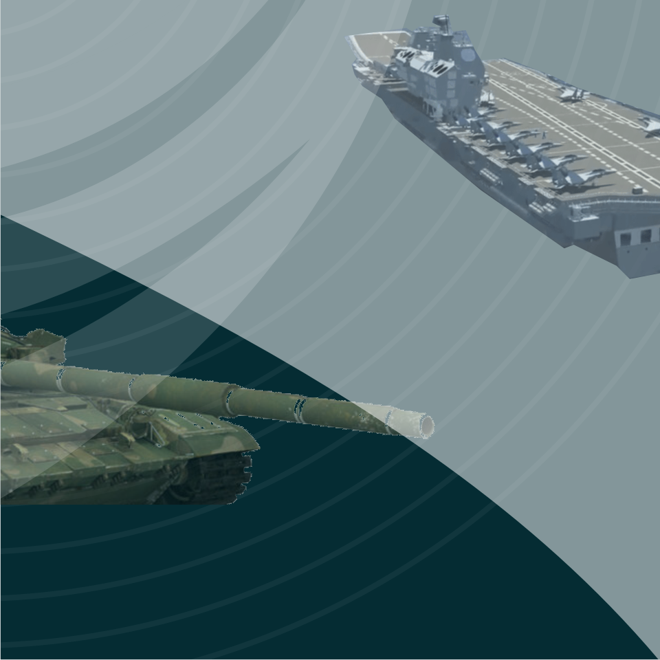
Defence
Trusted partner of Defence organization
Naval
Trusted Partner of Naval Application
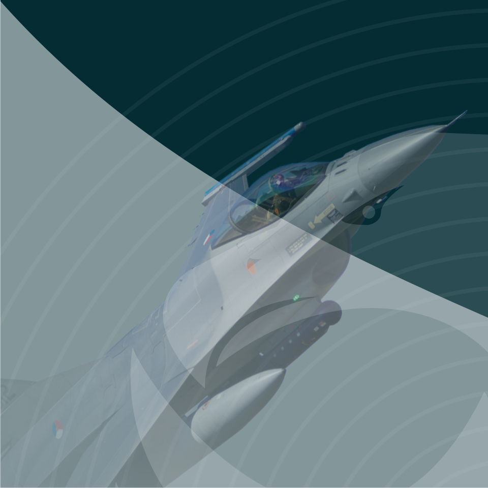
Air Borne
Trusted partner of Air Borne Applications
Homeland
Trusted partner of Safe & Smart cities


